Suppressing excessive noise from 22 GHz retimer chips was one matter. Pinpointing the optimal characteristics of a desired solution was another. Read how a global networking technology manufacturer compared nine different simulations and selected Laird™ Eccosorb™ GDS as its ideal, Laird laboratory-confirmed high frequency absorber to reduce total radiated power.
Simulations Help Identify “Sweet Spot” Microwave Absorber Material for Noisy Retimer and ASIC Chips
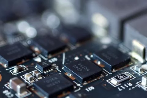
Server router boards are home to a range of retimer and application-specific (ASIC) chips. Although both chips are sources of troublesome radiated emissions, laboratory simulations now point to solutions which will reduce unwanted noise and improve overall signal integrity.
In one case at a global networking technology company, retimers functioning at 22GHz transmit fresh copies of signals yet are prone to excessive noise. Initially, gasketing was used to partially suppress retimer and ASIC noise evident in the 20 to 30 GHz frequency range. As data speeds increased, gaskets proved inadequate. The company had also considered metal shielding. However, in router board locations where the heat sink was larger than the chip, the energy would couple through the gap between the router board and heat sink. A novel solution was needed to suppress signal interference.
Evaluating absorber solutions
The company opted to decrease coupling by replacing gasketing with RF/microwave absorbers. The material would fit tightly to and surround retimer and ASIC chips in a “picture frame” configuration, thus improving attenuation of excess noise.
There were questions – and few specific answers. What would be the best, most effective absorber material to apply in terms of thickness, width, and type? How did changes in material parameters correlate to and affect the fight against excess noise at higher frequencies? What about a solution for lower frequencies?
For help, the company turned to the in-house simulation and modeling team at Laird, a DuPont business, and its Ansys HFSS full-wave 3D electromagnetic simulation software. Laird would use laboratory simulations to calculate reductions in total radiated power (TRP) and signal loss when evaluating different Laird absorbers with varying parameters.
Researchers weighed all variables: PCB and heat sink sizes, the distance between the PCB and heat sink, available board space, and absorber thickness and width, as well as magnetic loading. Goals included:
- Define the best absorber material for each frequency.
- Define TRP impact resulting from use of a specific absorber width.
- Define TRP impact resulting from use of a specific absorber thickness.
- Optimize width/thickness for a constant volume of absorber material.
- Pinpoint the best or “sweet spot” absorber and configuration across a range of different absorbers and parameters.
Testing various thicknesses
For example, researchers assessing one absorber, Laird™ Eccosorb™ BSR-1, evaluated TRP reduction effectiveness with absorber thickness set at 2 mm, at 1.6 mm, and lastly at 1 mm. Results indicated a clear improvement in TRP reduction over all frequencies with the use of thicker absorbers. The simulation on the thickest BSR-1 absorber (1 mm) showed it achieved the most effective TRP result: an approximate 17db drop in TRP at 22 GHz.
Evaluating assorted widths
Working more with BSR-1, Laird researchers then used simulations to determine the best absorber width to effectively reduce TRP. Using a 1.6 mm thickness as a baseline, BSR-1 absorber widths were set at 1 mm, at 3 mm, at 5 mm, and lastly at 7 mm. The added width paid off: The 7 mm (about 0.28 in. wide) simulation was most effective, delivering a 15db reduction in TRP at 22 GHz.
Thickness vs. Width: Which is more important?
Maintaining a constant volume of absorber material and across all parameters, researchers reached two significant conclusions of high interest to this networking technology company:
- At lower frequencies, absorber thickness is more important for optimal TRP reduction.
- At higher frequencies, absorber width is more important.
Best performing absorber material
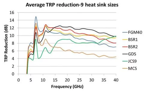
To account for differences in PCB/heat sink and absorber size, and to better determine the average reduction in TRP, Laird simulated a total of nine sizes and separations. The three most significant findings of these simulations were:
- At lower frequencies (less than 20 GHz), Laird™ Eccosorb™ FGM-40 and two Laird™ Eccosorb™ BSR absorbers performed the best overall at reducing TRP.
- At higher frequencies found most frequently in retimer and ASIC chips (greater than 20 GHz), Laird™ Eccosorb™ GDS performed the best overall at reducing TRP.
- At frequencies greater than 40 GHz, Laird™ Eccosorb™ JCS-9 proved the best.
A proven absorber solution for high-frequency applications
Faster data transfer rates demand comprehensive, proven solutions to mitigate radiated emissions. In the retimer and ASIC high frequency applications described here, Laird Eccosorb™ GDS exhibits high permittivity and permeability for dampening cavity resonances. This absorber and other products from Laird are now designed-in by the company. Its design team has requested no additional simulations because Laird’s initial work continues to guide decisions. Most recently, Laird has installed a novel compression molding manufacturing process for its picture frame absorber. Compression molding benefits the company through lower material costs and achieving 0.50 mm (about 0.02 in.) absorber tolerances. With this custom solution in place, this networking technology company successfully suppresses signal interference in its retimer and ASIC high frequency applications, which facilitates ongoing innovation that benefits its customers.